Chemical Vapor Deposition
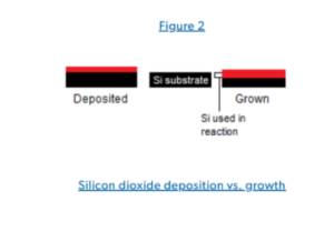
Chemical vapor deposition (CVD) oxide is a linear growth process where a precursor gas deposits a thin film onto a wafer in a reactor. The growth process is low temperature and has a much higher growth rate when compared to thermal oxide. It also produces much thinner silicon dioxide layers because the film is deposted, rather than grown. This process produces a film with a high electrical resistance, which is great for use in ICs and MEMS devices, among many other applications.
Chemical vapor deposition (CVD) oxide is performed when an external layer is needed but the silicon substrate may not be able to be oxidized.
Chemical Vapor Deposition Growth:
CVD growth occurs when a gas or vapor (precursor) is introduced into a low temperature reactor where wafers are arranged either vertically or horizontally. The gas moves through the system and distributes evenly across the surface of the wafers. As these precursors move through the reactor, the wafers begin to absorb them onto their surface.
Once the precursors have distributed evenly throughout the system, chemical reactions begin along the surface of the substrates. These chemical reactions start as islands, and as the process continues, the islands grow and merge to create the desired film. Chemical reactions create biproducts on the surface of the wafers, which diffuse across the boundary layer and flow out of the reactor, leaving just the wafers with their deposited film coating.
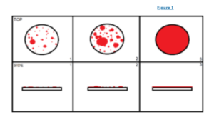
(1.) Gas/Vapor begins to react and form islands on substrate surface. (2.) Islands grow and begin to merge together. (3.) Continuous, uniform film created.
Benefits of Chemical Vapor Deposition:
- Low temperature growth process.
- Fast deposition rate (especially APCVD).
- Does not have to be a silicon substrate.
- Good step coverage (especially PECVD).
Types of CVD
LPCVD
Low pressure chemical vapor deposition is a standard chemical vapor deposition process without pressurization. The major difference between LPCVD and other CVD methods is deposition temperature. LPCVD uses the highest temperature to deposit films, typically above 600°C.
The low-pressure environment creates a very uniform film with high purity, reproducibility, and homogeneity. This is performed between 10 – 1,000 Pa, while standard room pressure is 101,325 Pa. Temperature determines the thickness and purity of these films, with higher temperatures resulting in thicker and more pure films.
PECVD
Plasma enhanced chemical vapor deposition is a low temperature, high film density deposition technique. PECVD takes place in a CVD reactor with the addition of plasma, which is a partially ionized gas with a high free electron content (~50%). This is a low temperature deposition method that takes place between 100°C – 400°C. PECVD can be performed at low temperatures because the energy from the free electrons dissociates the reactive gases to form a film on the wafer surface.
This deposition method uses two different types of plasma:
- Cold (non-thermal): electrons have a higher temperature than the neutral particles and ions. This method uses the energy of electrons by changing the pressure in the deposition chamber.
- Thermal: electrons are the same temperature as the particles and ions in the deposition chamber.
Inside the deposition chamber, radio-frequency voltage is sent between electrodes above and below the wafer. This charges the electrons and keep them in an excitable state in order to deposit the desired film.
There are four steps to growing films via PECVD:
- Place target wafer on an electrode inside the deposition chamber.
- Introduce reactive gases and deposition elements to the chamber.
- Send plasma between electrodes and apply voltage to excite the plasma.
- Reactive gas dissociates and reacts with the wafer surface to form a thin film. Byproducts diffuse out of chamber.
APCVD
Atmospheric pressure chemical vapor deposition is a low temperature deposition technique that takes place in a furnace at standard atmospheric pressure. Like other CVD methods, APCVD requires a precursor gas inside the deposition chamber, then the temperature slowly rises to catalyze the reactions on the wafer surface and deposit a thin film. Due to the simplicity of this method, it has a very high deposition rate.
- Common films deposited: doped and undoped silicon oxides, silicon nitrides. Also used in annealing.
HDP CVD
High density plasma chemical vapor deposition is a version of PECVD that uses a higher density plasma, which allows the wafers to react with an even lower temperature (between 80°C-150°C) within the deposition chamber. This also creates a film with great trench fill capabilities.
SACVD
Subatmospheric pressure chemical vapor deposition differs from other methods because it takes place below standard room pressure and uses ozone (O3) to help catalyze the reaction. The deposition process takes place at a higher pressure than LPCVD but lower than APCVD, between about 13,300 Pa and 80,000 Pa. SACVD films have a high deposition rate, which improves as temperature increases until about 490°C, at which point it begins to decrease.
- Common films deposited: BPSG, PSG, TEOS.
USG, BPSG
Undoped Silicate Glass – USG
Undoped silicate glass has a high deposition rate at low temperatures and has similar properties to silicon dioxide. This means it is easy to deposit via plasma enhanced CVD (PECVD), HDP-CVD or SACVD. It’s most common as an insulator and passivation layer in multilevel IMD applications.
Borophosphosilicate Glass – BPSG
Borophosphosilicate glass (BPSG) is a coating made from a mixture of oxygen and hydrides of silicon (silane – SiH4), boron (diborane – B2H6), and phosphorus (phosphine – PH3). It is also called a doped oxide film because it is similar to silicon dioxide with the addition of boron and phosphorus, which change its thermal properties. The addition of hydrides drastically lowers the melting point of glass, which make this process very useful when a wafer has limited thermal capabilities.
BPSG is applied to wafers via different chemical vapor deposition (CVD) techniques. The most effective and common deposition technique is PECVD, although other CVD processes will also work. Atmospheric pressure CVD (APCVD), subatmospheric pressure CVD (SACVD), low pressure CVD (LPCVD) and high density plasma CVD (HDP-CVD) are some of the other CVD processes that will apply BPSG to a wafer.
The ratio of oxygen to hydrides in the deposition chamber is usually between 40:1 and 60:1, which significantly lowers the deposition temperature of BPSG when compared to other doped oxide films. To deposit these films, the furnace temperature is 360°C – 390°C , with an optimal deposition temperature of around 370°C.
In order to ensure these wafers will properly insulate inter-metal dielectrics and maintain their high flatness qualities, these wafers often undergo a process called ‘reflow’, which takes place either in a furnace or through rapid thermal annealing (RTA). Because of their temperature sensitivity, these wafers are not subject to temperatures above 900°C to prevent damage and imperfections. This also means RTA is performed at a lower temperature.
Borophosphosilicate glass protects the underlying silicon substrate and conductive paths in semiconductors and helps with device planarization. This makes BPSG most valuable in semiconductor device fabrication, inter-metal dielectrics (IMD), and pre-metal dielectrics (PMD).